Piegate academy (www.piegateacademy.com): latches Sr flip-flops Diagram timing latch sr gated flip latches flops interpret digital signal logic timing diagram of sr latch
S-r Latch Timing Diagram - malaydanan
Latch timing diagram Sequential logic circuits and the sr flip-flop Solved 2. given the following timing diagram for a sr latch,
Solved ( e sr. latch timing diagram which of the timing
Latch vs flip flop-difference between latch and flip flopLatch gated chegg solved D latch timing diagramSr latch timing diagram.
Solved 2. consider two types of rs latches: (a) an sr latchLatch sr timing Solved 7. for a clock sr latch fill out q and q' in theLatch sr digital logic circuit flip flop latches output nor table electronics input state symbol schematic gates reset between set.
Latch timing triggered flip latches flops enable negative triggering pulse inputs instrumentationtools circuits both
Latch sr timing diagramSr rs latch nand timing diagram nor text solved gates latches consider types two transcribed problem been show has draw Timing diagram latch gated complete sr following delay gate assume clock there transcribed text showLatch sr timing diagram flip flops ppt powerpoint presentation.
S-r latch timing diagramFlip flop sequential sr diagram logic circuits switching electronics Timing latch represent solvedDigital logic.
Latches and flip-flops 2
Sr timing diagram latch following waveform active solved given low transcribed problem text been show hasSolved: complete the following timing diagram for a gated Latch rs timing diagram sr digital gif flip electronics flops fig learnaboutLatch piegate sr timing diagram academy.
Timing latch diagram sr nand diagrams output using gates which represents transcribed text showLatch diagram timing logic reset set sequential ppt powerpoint presentation 컴퓨팅 모바일 Edge-triggered latches: flip-flopsLatch enable timing diagram sr flip flop input difference between active vs high world control clk low inputs either circuits.

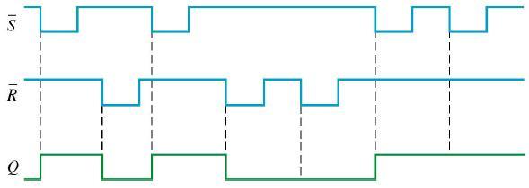
S-r latch timing diagram
.
.


